


Tutorials
Tutorial I – Unlocking Material-to-System Innovation with AI
Hussam Amrouch – Technical University of Munich, Germany
We are entering a transformative era where AI is not only advancing our understanding of the world but also might revolutionize the design and development of semiconductor technologies and chip design. As technology scaling faces fundamental physical and reliability challenges, a holistic, material-to-system co-optimization approach is becoming essential. In this keynote, we explore how AI can serve as a unifying force across the semiconductor design stack—from material and device optimization to system-level implementation. We demonstrate how AI algorithms can accelerate device physics simulations, enable faster development of transistor compact modeling, and offer unprecedented speed in standard cell library characterization. We highlight how AI empowers designers, for the first time, to capture and propagate awareness of aging- and defect-related phenomena—originating at the material and device level—all the way to GDSII and final sign-offs. We further discuss the critical importance of AI-driven methodologies in emerging domains such as emerging non-volatile memories and cryogenic CMOS, where the assumptions of classical semiconductor modeling break down. Finally, we demonstrate how neural networks can be effectively employed in transistor compact model offering unprecedented speedup in SPICE simulations with an accuracy error of below 0.1%.
Hussam Amrouch is a Professor heading the Chair of AI Processor Design at the Technical University of Munich. He is the Founding Director of the Munich Advanced-Technology Center for AI Chips (MACHT-AI). He is the head of the Semiconductor Test and Reliability at the University of Stuttgart, Germany. He is the Academic Director of TU Munich Venture Lab for Semiconductor. He is the head of the Brain-inspired Computing at the Munich Institute of Robotics. He received his Ph.D. degree with the highest distinction from KIT, Germany, in 2015. He has over 330 publications, including over 135 journal articles. His multidisciplinary research covers semiconductor device physics, chip design, and computer architecture. His research interest is design for reliability, AI acceleration, emerging technologies, in-memory computing, and cryogenic circuits for quantum computing. His research in AI chips and reliability has been funded by DFG, Bavarian Ministry of Economy, Bavarian Ministry of Science, Federal Ministry of Science, Advantest, Infineon, and the U.S. Office of Naval Research.

Tutorial II – Energy efficient power switches with Gallium Nitride technology
Srabanti Chowdhury – Stanford University, USA
GaN technology is an ever-expanding topic of research and development, proving its potential to solve several challenges in power conversion that cannot be addressed by Si. For instance, medium voltage (650-900V) devices using the HEMT configuration have been able to reduce form factor at the system level by driving circuits at higher frequencies (100KhZ-1Mhz) and eliminating heat sinks or reducing cooling requirements. This alone sparked the interest in GaN research to save space, energy and ultimately cost of power conversion. However, in power conversion the demand of high current from a single chip for a rated voltage is a standard need. Particularly when the market is favorable towards electrification of cars and other means of transportations, GaN must expand its scope to provide high power solutions with higher power density compared to Si, and even SiC. Vertical devices have been the choice of power device engineers for economic use of the material and maximum use of its physical properties (which allow highest possible blocking field, field mobility, etc.). GaN vertical devices, therefore, carry all the advantages offered by vertical geometry and are being explored increasingly with emphasis on material and device needs.
An overview of the achievements in vertical Gallium Nitride (GaN)-based power electronic devices will be presented with particular reference to a current aperture vertical electron transistor (CAVET), MOSFETs), Static Induction Transistor (SIT), and high voltage diodes.
Prevalent opinion suggests GaN HEMTS are suitable for 650V, while vertical devices are more suited for 1.2kV and up. In this tutorial I would build an argument to suggest how the overall (most likely system-level, but also device-level) cost would decide whether lateral or vertical devices would be the ultimate solution for power deices. Avalanche breakdown observed due to impact ionization of carriers in vertical devices is a key reason to help make a case for the superiority of vertical devices.
Srabanti Chowdhury is a Professor in the Department of Electrical Engineering at Stanford University, with a courtesy appointment in Materials Science and Engineering. She specializes in semiconductor device engineering and leads Stanford’s Wide Bandgap (WBG) Lab, where her research focuses on power conversion, delivery and advanced thermal management for computation and RF systems.
She received her Ph.D. in Electrical and Computer Engineering from the University of California, Santa Barbara, in 2010. Her honors include the 2025 Quantum Device Award for pioneering contributions to vertical gallium nitride transistors and phonon-engineered interfaces; the 2023 SRC Technical Excellence Award for contributions to thermal interfaces; the 2020 Alfred P. Sloan Fellowship in Physics; and the 2016 Young Scientist Award at ISCS, along with several other early-career recognitions. She is a Fellow of the IEEE and a Senior Fellow of the Precourt Institute of Energy at Stanford University. Her lab is committed to research that directly advances energy efficiency, as well as to training the next generation of engineers and scientists to address critical challenges in energy and electronics.

Tutorial III – Reliability of Silicon-based Transistors processed at low temperatures
Xavier Garros – CEA-Leti, France
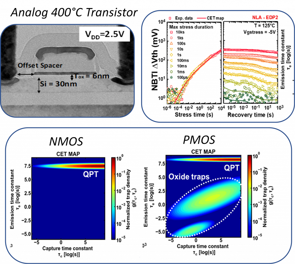
3D Sequential Integration (3DSI) is a promising alternative to continued technology scaling, enabling energy-efficient and cost-effective circuit design through the sequential stacking of active device layers. A key challenge, however, is the requirement for low-thermal-budget processing to preserve the integrity of underlying layers. This constraint raises concerns regarding the reliability of low-temperature transistors and remains a major barrier to large-scale adoption. This tutorial revisits the critical challenges associated with meeting reliability requirements for low-temperature silicon-based CMOS transistors, with a primary focus on bias temperature instability (BTI) in both n- and p-MOSFETs for digital and analog applications. A systematic investigation of the impact of thermal budget on BTI will be presented, highlighting a distinct transition in BTI behavior for processing temperatures below 600 °C. Advanced characterization and modeling techniques, including the CET map approach, will be employed to identify the oxide traps responsible for BTI in both device types. We will benchmark several process optimization strategies aimed at improving low-temperature oxide quality, including oxide growth methods, gate-stack engineering (TiN versus polysilicon), and post-deposition curing treatments such as hydrogen annealing and nanosecond laser annealing (NLA). Finally, hot-carrier reliability will be examined, with particular emphasis on the role of oxide traps in low-k spacers.
Xavier Garros is a Senior Scientist in the Silicon Technologies Department at CEA-LETI. He received his Ph.D. from the University of Marseille, France, in 2004, with a focus on the physics and electrical properties of high-k dielectrics. His expertise spans electrical characterization, device physics, and reliability modeling in advanced CMOS technologies, including bulk, FDSOI, and nanowire devices. He is currently involved in the development of 3D monolithic integration and RF technologies. He has supervised 10 Ph.D. theses and is the author or co-author of five patents and more than 160 publications in international journals and conferences in the field of CMOS physics. He has also served on the technical program committees of leading international conferences, including IEDM, IRPS, and SISC.
Tutorial IV – CMOS product yield and reliability risk: Plasma Induced Damage (PID) past, present and future nodes
Andreas Martin – Corporate reliability department, Infineon Technologies AG, Germany
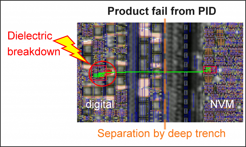
Plasma processing-induced charging damage (PID) is a significant yield and reliability risk for integrated circuits. A vast number of investigations have been published since the early 1990s. Prevention of PID is typically achieved through thorough process qualification and comprehensive design-rule definitions. However, in recent years, product failures related to PID have been reported in the literature for state-of-the-art technologies featuring highly isolated well configurations and complex, large-area circuits. This indicates an urgent need for refined PID design rules, which have not yet been fully adopted across the semiconductor industry.
This tutorial will present the background of PID and highlight the various failure modes associated with specific process options and circuit configurations. Examples supported by experimental data will be provided, and safe design areas for circuit designers will be defined. All topics will be discussed with reference to key publications from major international journals and conferences.
Content:
- Introduction: basic degradation mechanisms
- Degradation and charge trapping in dielectric layers
- Failure modes
- Metal interconnects at the gate electrode
- Metals at source, drain, and well regions in SOI technologies
- Well charging in isolated wells
- MIM capacitor degradation
- Impact of PID on metallization processes
- Detection and characterization of PID
- Circuit-level protection against PID
- Design-rule checks for products
- Standardization efforts
- Outlook: PID in advanced technology nodes
Andreas Martin received his master´s degree in electronic & electrical engineering from the Technical University of Darmstadt, Germany. He worked in Tyndall Research Institute in Cork, Ireland for several years with a focus on CMOS gate oxide reliability, before he started in 1998 in the corporate reliability department with Infineon Technologies AG in Munich, Germany. Since then, he develops methodologies for plasma induced damage (PID) reliability qualification and fast wafer-level reliability (fWLR) monitoring for technology nodes in-house and for the foundry business. He is in the lead for PID qualification methodology and antenna design rule development at Infineon Technologies AG. He has served in the JEDEC 14.2 committee for over 25 years, where he is currently chair of the 14.2 committee and moderates three task groups: TG142_3 development of a standard on the qualification of PID gate antennas, TG142_10 standard on qualification of PID well charging, TG142_2 guideline on productive fWLR Monitoring.

Tutorial V – Degradation Physics and Degradation Rate Modeling
Joe W. McPherson – McPherson Reliability Consulting LLC, USA
Degradation physics is very important because materials degradation is a precursor to device failure. Understanding the degradation rate permits the reliability engineer to predict time-to-failure (TF) without the lengthy time required to actually measure TF. More importantly, degradation rate modeling permits the user to take corrective action before device failure actually occurs. The goal of degradation-rate modeling is to produce zero actual failures! Zero failures are incredibly important where semiconductor related materials play essential roles in our life-support systems (fully autonomous driving vehicles, implantable medical devices, traffic controllers, space travel, etc.).
All fabricated materials are metastable and will degrade with time. This is a consequence of the material changing in an effort to reach a lower Gibbs Potential. For semiconductor-related materials, degradation is normally recorded at the macroscopic level (resistance increases, leakage increases, threshold voltage increases, etc.) but the root-causes of degradation may need to be understood at the microscopic/molecular level. For any material to be successful/reliable in its intended application, the material degradation rate (as a function of use conditions: voltage, temperature, environment, etc.) must be fully comprehended. Toward this end, it is very important to understand when macroscopic models can no longer be used and a more microscopic (molecular/quantum) approach must be used for nanomaterials degradation. During this tutorial, we will investigate degradation physics and degradation rate modeling for several very important semiconductor-related failure mechanisms: time-dependent dielectric breakdown (TDDB), hot-carrier injection (HCI), bias temperature instability (BTI), electro-migration (EM), and stress migration (SM).
Joe McPherson holds a PhD degree in Physics and is an IEEE Fellow. He is widely recognized as an expert in Reliability Physics & Engineering. He has published over 200 papers on reliability physics and awarded 30 patents. He authored a reliability textbook that is widely used by students and practicing engineers: Reliability Physics and Engineering, Springer Publishing (now in its 3rd Edition, 2019). Presently, Joe is Founder & CEO of McPherson Reliability Consulting, LLC.

Tutorial VI – Introduction to SiC power MOSFET technology and reliability
Peter Moens – onsemi Power Solutions Group, Belgium
In this tutorial we will cover the basic aspects of both planar and trench gate SiC power MOSFET device technology and their reliability. The aim is to provide the audience with insight into the status of the reliability of SiC power devices. The following topics will be addressed:
- Characterization of the SiC/SiO2 interface by charge pumping and ultra-fast BTI measurements. From the latter the capture and emission time constant maps are derived.
- Identification of the physical nature of the interface point defects through electrically detected magnetic resonance (EDMR)
- Gate Switching instability
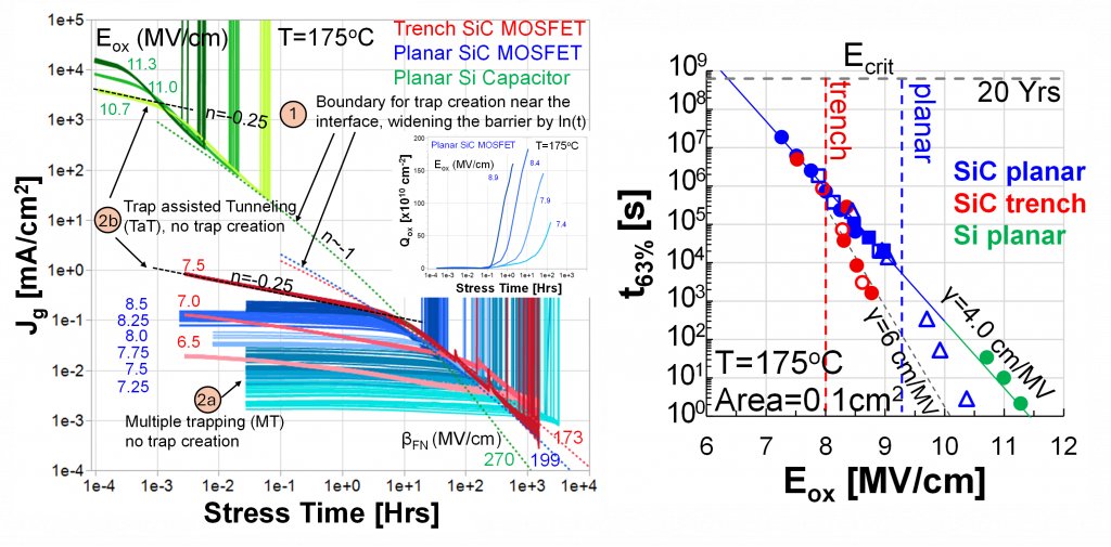
- Gate oxide reliability (TDDB) and lifetime. Comparison of SiC/SiO2 to Si/SiO2
- Reverse bias reliability
- Cosmic ray susceptibility
- Short circuit withstanding time
- Bipolar degradation
Finally, we will provide an outlook to “Moore’s law for power devices” and where we believe SiC will be heading into the future.
Peter Moens received a Master in nuclear physics and a Ph.D. in solid state physics from the University of Gent, Belgium, in 1990 and 1993 respectively. At onsemi is working on SiC MOSFETs. He is/was a member of the technical program committees of IEDM, ISPSD, IRPS, CSMANTECH, ICSCRM, IRW, EDTM, ESSDERC and ESREF. He was the General chair of ISPSD 2012. He authored and co-authored over 200 publications in peer-reviewed journals or conferences, 20 invited papers, and is the recipient of 6 best paper awards (including 2 ISPSD best paper awards as first author). He presented tutorials at IRPS, ISPSD, and EDTM. He is an inductee of the ISPSD International Hall of Fame. He holds 62 US patents.