





Invited Talks
Invited Talk I – Enabling Large Scale Implementation of Reliable WBG Devices from a Manufacturer’s Viewpoint
Dr. Stefano Aresu – Infineon Technologies, Austria
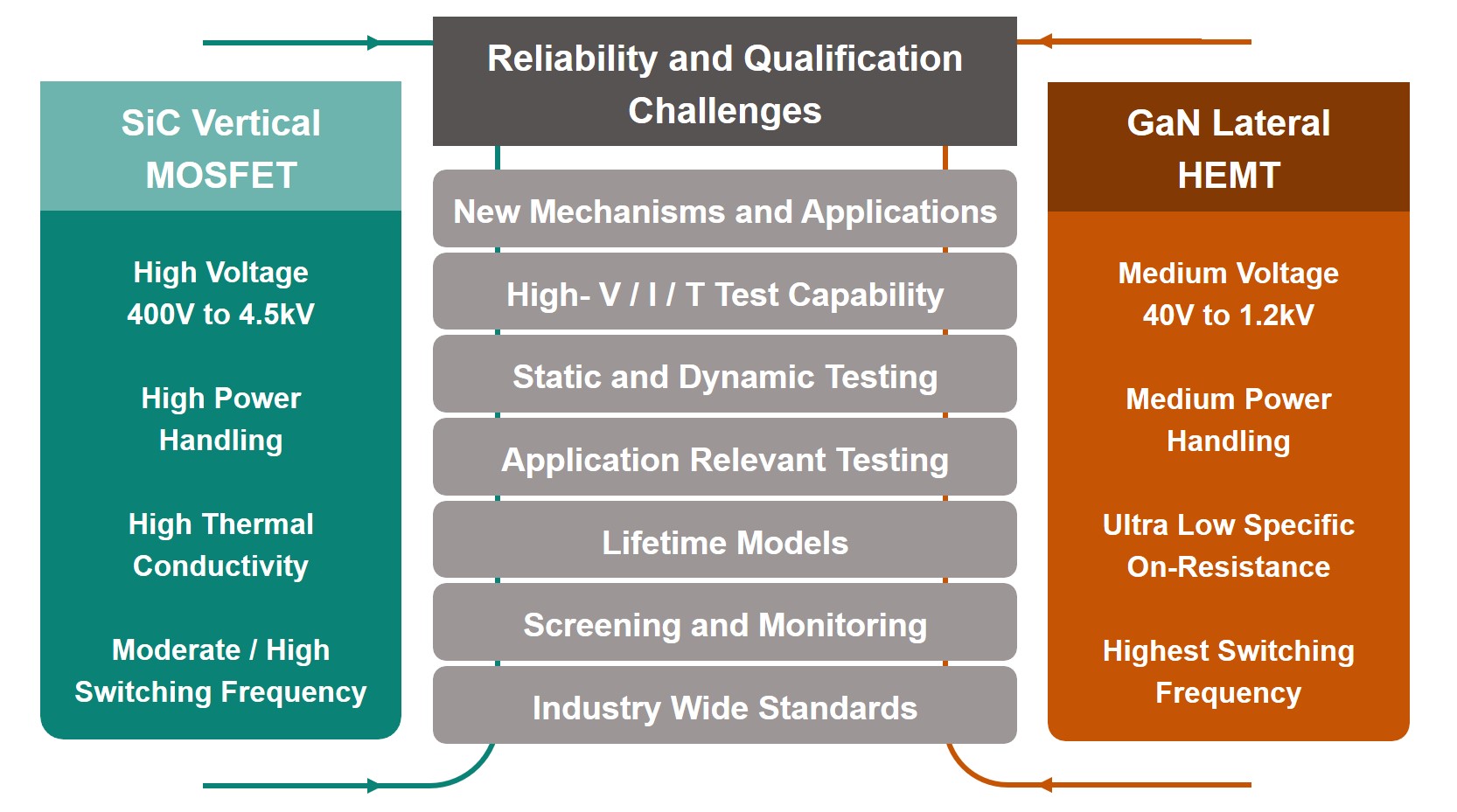
Wide bandgap (WBG) power semiconductors give significant advantages, but they also introduce new reliability risks and qualification demands. This talk highlights the challenges specifically shared by SiC Vertical MOSFETs and GaN Lateral HEMTs. Understanding the reliability limits of both technologies is important to meet the low-DPPM levels expected by customers and already achieved by mature Silicon MOSFETs. Dedicated dynamic measurements are needed to reveal new degradation mechanisms and develop related failure models. In addition, there is the desire to provide universal degradation models for each technology to be applied to a large portfolio of products with a variety of designs and application relevant needs. These insights shape our qualification strategy as a company and the demand for tailored industry-wide WBG standards. Managing extreme thermal and electrical stress during dynamic testing is particularly challenging, but it is important to balance manufacturing constraints with strict reliability targets. The SiC Vertical MOSFET shows its advantages in high-voltage and high-power applications, leveraging high thermal conductivity and moderate-to-high switching frequencies. We review its primary degradation mechanisms and discuss reliability tests used to evaluate its robustness under realistic operating conditions. Particular attention is given to gate oxide degradation, interface state generation, threshold voltage instability, and degradation induced by repetitive switching stress. While high temperature blocking condition and gate stress are primarily used to assess static reliability and gate oxide robustness, gate switching stress and other dynamic tests are essential for investigating mechanisms that arise under application-relevant switching conditions, as well as for defining production screening limits and guard bands to ensure the highest quality. Similar to the SiC MOSFET, the GaN Lateral HEMT requires also dynamic testing to capture degradation occurring only under switching stress. GaN devices show their advantages for medium-voltage and medium-power applications with their ultra-low specific on-resistance and ultra-high switching frequencies. Operating under extreme conditions introduces degradation mechanisms that a traditional qualification strategy may not reveal. Characterizing these mechanisms can ensure high reliability for large-scale deployment.
Dr. Stefano Aresu received his degree in electronic engineering from the University of Cagliari in 2000. He then joined IMEC, where he focused on hot carrier effects in power devices. After earning his Ph.D. in physics in 2005, he joined the Central Reliability Department at Infineon Technologies as a Reliability Engineer responsible for qualifying automotive and industrial power devices. His research included investigations on NBTI and hot carrier effects as well as the development of device life time models. Over the past few years, he has been responsible for process qualifications and transfers for advanced smart power technologies. As a Lead Principal Engineer, he currently serves as the overall coordinator for front-end reliability topics, implementing methods ranging from single devices to full products, including eFlash and RRAM memories. He is the author and co-author of over 30 papers and patents in microelectronics reliability and actively contributes to JEDEC and AEC-Q100 standards.
Invited Talk II – Cryogenic low-noise amplifiers for quantum computing: Engineering noise and thermal properties
Cezar Zota – IBM Research Europe, Switzerland
Cryogenic low-noise amplifiers are essential parts of today’s quantum computers and are primarily employed in the readout path at the 4 K stage to read the qubit states. Their performance and reliability directly impact the quantum computations, e.g. through the readout fidelity. As one of the few active, i.e. power-dissipating, cryogenic devices used already today, there are strict requirements placed in terms of noise-levels, power, stability and robustness. To support ever increasing qubit numbers, improved amplifiers will be desirable in the future. In this presentation, we demonstrate our cryogenic III-V high-electron mobility transistor technology based on the InGaAs/InP system. We show how noise properties depend on temperature, and how this dependence arises from various traps and defects across the heterostructure that can be effectively suppressed with quantum well engineering. We also describe thermal effects, in particular self-heating, which is one of the primary limits of noise and reliability in these devices. Several self-heating measurement methodologies are examined, such as quantum thermometry, which is able to determine both the intrinsic electron temperature as well as associated scattering mechanisms throughout the device self-heating process. Power semiconductors are vulnerable to thermo-mechanical stress due to the use of solid-metal interconnect technologies such as wire bonding, soldering, and sintering. This presentation showcases a successful usage of room-temperature Gallium-based liquid-metal pastes for chip-level packaging of SiC MOSFETs. All chip-critical interconnects (die-attach, topside, and gate connections) are implemented using liquid-metal, which remains liquid during operation. We tested the SiC MOSFETs for thermal and reliability performance. Liquid-metal packaged SiC MOSFETs showed improved thermal performance and an order of magnitude increase in power cycling lifetime. Notably, the liquid-metal pastes are contained without the use of any encapsulation.
Dr. Zota received the PhD degree in Electrical Engineering from Lund University, Sweden, in 2017. Since then, he has been a Staff Research Scientist and Master Inventor at IBM Research Europe – Zurich. His research interests include cryogenic electronics for quantum computing, including III-V amplifiers, cryo-CMOS, and cryogenic modelling. More recently, his work has also focused on state-of-the-art CMOS technologies, in particular for the back-end-of-line. He is the recipient of an Ambizione career grant from the Swiss National Science Foundation, is a member of the National Centre of Competence in Research SPIN, has coordinated several European research projects, and holds over 20 patents and has co-authored over 80 peer-reviewed publications in the field of electron devices.

Invited Talk III – Automotive Battery Management Chipset, In-field, Maintenance & Lifetime
Wenzel Prochazka – NXP Semiconductors Austria GmbH
High precision voltage measurements qualified for >15 years, backed with a safety certified system layout, cybersecurity and combined with cost effective wireless capability, are needed for modern EV powertrains to meet customer expectations. NXP’s Battery Management Chipset reference design supports maximizing battery longevity by combining multiple technologies not only as begin-of-life datasheet specifications. This presentation gives some insights into how we can achieve this.
With nearly 20 years background in EV Battery and powertrain development activities, Dr. Wenzel Prochazka joined NXP in 2023 to manage the electrification system products elaboration. Today he manages the process of NXP systems for HV batteries and enabling customers of NXP with a large part of the value share in innovative system solutions in processing and analog controls for HV EV powertrains.

Invited Talk IV – Picosecond Pulse Generation Methods for Die-to-Die ESD Testing
Christian Herpers – Fraunhofer EMFT (and Technical University of Munich)
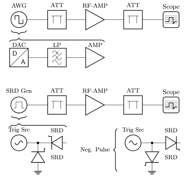
Due to miniaturization and heterogeneous integration of chiplets in the semiconductor industry, a need for electrostatic discharge (ESD) testing of die-to-die (D2D) interfaces has emerged. Current ESD testing methods, such as transmission line pulsing with switching relays, cannot reliably replicate fast D2D ESD events. Hence, novel pulse generation schemes reducing the transition time to below 50 ps are required. This work presents two methods of picosecond pulse generation with broadband radio-frequency amplification for D2D ESD testing. A high-speed arbitrary waveform generator is leveraged to generate short pulses achieving transition times down to 6.4 ps and amplitudes up to 28 V after amplification. Pulse generation with step recovery diodes yields transition times below 30 ps and amplitudes up to 19 V after amplification. While pulse generation with step recovery diodes is simple, less costly, and yet effective, the approach using high-speed arbitrary waveform generation shows overall better results. The presented pulse generation methods can be applied to future ESD testing of D2D interfaces in heterogeneously integrated devices.
Christian Herpers received his B.Eng. in electrical engineering and information technology from the Munich University of Applied Sciences, Munich, Germany, in 2022 and completed his M.Sc.E. in electrical engineering at the University of New Brunswick, Fredericton, NB, Canada, in 2023. From 2017 to 2022, he was a Dual and Working Student with Rohde & Schwarz, Munich and from 2022 to 2023, a Research and Teaching Assistant with the University of New Brunswick. Since 2024, he has been with the Technical University of Munich and joined the Fraunhofer EMFT Institute for Electronic Microsystems and Solid State Technologies as a Research Assistant in 2025. His research interests include electrostatic discharge, RF measurements, and wireless power.
Invited Talk V – From Device Reliability to System Reliability: Challenges Across the Photonics Value Chain
Michael Rogers – ams OSRAM AG, Austria
Digital photonic products are increasingly complex systems comprising semiconductor devices, optical post-processing layers, advanced packaging technologies, interconnect structures, and optoelectronic assemblies. While significant progress has been made in understanding the reliability of individual photonic components—including LEDs, VCSELs, photodiodes, and SPADs—industrial experience shows that many field reliability issues originate from downstream processing, component integration, and system-level interactions. This presentation examines reliability from a broader product perspective, addressing the complete photonics value chain, from device fabrication to long-term performance in end applications. Particular emphasis is placed on reliability risks introduced during downstream processing and system integration. Examples include silicon post-processing technologies such as through-silicon vias (TSVs), color and interference filters, handling- and assembly-induced defects, interconnect degradation, corrosion phenomena, contamination effects, and package-induced thermomechanical stresses. These mechanisms can create latent defects or accelerate degradation processes that become apparent only during prolonged environmental exposure or field operation. Through selected industrial examples, the presentation illustrates how reliability risks evolve and propagate across increasingly integrated photonic products. Particular attention is given to the interfaces between semiconductor devices, optical post-processing layers, interconnect technologies, packaging elements, and other structural components of the system architecture. The discussion demonstrates how interactions among these elements can create complex failure paths that may not be evident when components are assessed in isolation. In some cases, system-level reliability requirements and integration-related failure mechanisms ultimately necessitate changes to the design of individual components, highlighting the strong interdependence between device design and product architecture. Building on these observations, the presentation highlights the importance of understanding the physical architecture of photonic systems. Reliability risks frequently originate at interfaces where optical, electrical, thermal, mechanical, and environmental sensitivities interact, creating cross-dependencies that may remain hidden when components are evaluated independently. A thorough understanding of component sensitivities, interface behavior, and resulting cross-dependencies is therefore essential for identifying and mitigating system-level failure mechanisms. Risk-management methodologies such as DFMEA are valuable tools, but their effectiveness ultimately depends on a sound understanding of the underlying architecture and interaction mechanisms. This broader perspective supports a shift from a purely component-centric view of reliability toward a system-level understanding of photonic products. By linking physical degradation mechanisms to architectural interfaces and component interactions, reliability can be assessed in terms of customer-relevant outcomes such as sensitivity loss, accuracy degradation, parametric drift, reduced signal-to-noise ratio, or catastrophic failure. This perspective provides a more effective framework for identifying and mitigating reliability risks in increasingly integrated photonic systems. While component reliability remains the foundation of robust photonic products, increasingly integrated systems demand a broader reliability perspective. Understanding system architecture, component interfaces, and integration-related interactions is essential for managing reliability risks and preserving functional performance throughout product lifetime. Meeting future challenges will require a holistic reliability approach spanning the entire photonics value chain—from device physics to system architecture.
Dr. Michael Rogers is Senior Director of Quality and Head of Technology Quality Engineering at ams OSRAM, where he is responsible for quality engineering in new technology development and leads the global reliability and failure analysis laboratories for the Light Sensing and Photonics business. He received a Diplomingenieur degree (equivalent to an MSc) in Technical Chemistry, a Doctorate in Technical Physics, and a Master of Advanced Studies in Nanotechnology and Nanoanalytics from Graz University of Technology. He began his career in electron microscopy and semiconductor failure analysis, specializing in focused ion beam (FIB), transmission electron microscopy (TEM), and advanced materials characterization. Since joining ams OSRAM in 2007, he has held roles spanning defect engineering, process integration, product reliability, and global quality and reliability leadership. His professional interests include semiconductor reliability, optical sensing technologies, failure analysis, and reliability engineering across the photonics value chain.
Invited Talk VI – Ultra-Reliable All-Liquid Interconnections for Power Electronics Components
Francesco Iannuzzo – Polytechnic of Turin, Italy

Power semiconductors are vulnerable to thermo-mechanical stress due to the use of solid-metal interconnect technologies such as wire bonding, soldering, and sintering. This presentation showcases a successful usage of room-temperature Gallium-based liquid-metal pastes for chip-level packaging of SiC MOSFETs. All chip-critical interconnects (die-attach, topside, and gate connections) are implemented using liquid-metal, which remains liquid during operation. We tested the SiC MOSFETs for thermal and reliability performance. Liquid-metal packaged SiC MOSFETs showed improved thermal performance and an order of magnitude increase in power cycling lifetime. Notably, the liquid-metal pastes are contained without the use of any encapsulation.
Francesco Iannuzzo is a professor of reliable power electronics with the Power Electronics Innovation Center (PEIC) at Politecnico di Torino, Italy. His research focuses on the reliability of wide-bandgap power devices (SiC MOSFETs, GaN HEMTs), their modeling and characterization, condition monitoring, simulation, and new driving concepts to improve reliability. Prof. Iannuzzo is the author or co-author of over 350 publications in journals and international conferences, five book chapters, and an edited book on Modern Power Electronic Devices. He has delivered over 50 technical seminars, keynotes, and several invited speeches on power electronic device reliability at top-tier conferences, including ISPSD, IRPS, EPE, ECCE, PCIM, and APEC. Furthermore, he is a Fellow of the U.S. Institute of Electrical and Electronics Engineers (IEEE). He has served as General Chair of ESREF 2018, IWIPP 2022 (International Workshop on Integrated Power Packaging), and EPE-ECCE Europe 2023.

Invited Talk VII – Active Auto Thinning (AAT): An AI-Driven Autonomous FIB Endpointing Method Based on Cut-Face Probability Inference and Image Interpolation for Advanced Memory Devices
Bryan Sang Hoon Lee – Micron Technology, USA
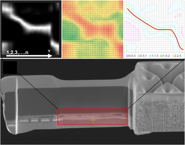
As semiconductor memory technologies continue to scale into the sub-10 nm regime, accurate endpoint determination during focused ion beam (FIB) thinning has become a critical challenge for transmission electron microscopy (TEM) sample preparation and failure analysis. Conventional passive auto thinning (PAT) workflows rely on predefined fiducials and operator interpretation of processed scanning electron microscopy (SEM) images, limiting endpoint precision and increasing susceptibility to process variability, beam instability, and human error. This study presents an autonomous FIB thinning methodology, termed Active Auto Thinning (AAT), that integrates machine vision, artificial intelligence (AI), probability-based endpoint prediction, and image interpolation algorithms for real-time control of FIB milling in advanced DRAM and NAND devices. The proposed framework utilizes sequential Slice-and-View SEM datasets to reconstruct three-dimensional device geometry and train AI models capable of recognizing evolving cross-sectional features as milling progresses. Rather than relying on image data optimized for human visualization, the system analyzes detector-derived information directly, preserving high-frequency structural information and enabling enhanced endpoint sensitivity. During operation, probability maps generated from real-time SEM images are combined with interpolation-based distance estimation to predict the remaining distance between the current cut face and the target region of interest. A closed-loop control architecture continuously updates process parameters and autonomously determines milling termination conditions. Experimental validation was performed using advanced FIB-SEM platforms and applied to leading-edge memory devices. The AAT workflow demonstrated reliable identification of target cut faces, robust compensation for beam and process variations, and autonomous operation without operator intervention. Compared with conventional PAT methods, AAT produced thinner and more uniform TEM lamellae, achieving specimen thicknesses near 10–20 nm while maintaining nanometer-scale endpoint accuracy. Statistical evaluation across multiple DRAM samples yielded an average lamella thickness of 15.3 nm with a 2σ variation of 1.26 nm and target-centering accuracy within 0.72 nm (2σ). The resulting TEM specimens exhibited reduced three-dimensional projection effects, improved critical-dimension metrology capability, and enhanced structural fidelity. The implementation of AAT represents a transition from automated to truly autonomous FIB sample preparation by enabling dynamic decision-making based on real-time image inference rather than fixed process scripts. The methodology improves throughput, repeatability, and data quality while reducing dependence on operator expertise. These results demonstrate the feasibility of AI-driven autonomous endpoint detection and establish a foundation for scalable, high-throughput semiconductor failure analysis and future unmanned laboratory environments.
Bryan Sang Hoon Lee is a Principal Engineer in the Yield Enhancement and Technology Laboratory at Micron Technology (USA), where he develops advanced failure analysis and characterization solutions for next-generation memory devices. His expertise includes focused ion beam (FIB) technologies, transmission electron microscopy (TEM), machine vision, and AI-driven process automation for advanced memory device applications. Prior to joining Micron in 2021, he spent a decade at FEI Company (now Thermo Fisher Scientific), contributing to advanced FIB/SEM technologies and materials characterization solutions. Dr. Lee holds M.S. and Ph.D. degrees in Materials Science and Engineering from Seoul National University and The University of Texas at Dallas. His recent work focuses on autonomous laboratory workflows and real-time process control. Dr. Lee has authored and presented numerous technical papers at international conferences, including ISTFA, commercialized multiple patented technologies, and continues to advance autonomous failure analysis technologies for semiconductor manufacturing.
Invited Talk VIII – Reaching the BTI 10yrs Lifetime for 2.5V BEOL Compatible (<420°C) High Voltage Si-CMOS
William Vandendaele – CEA-Leti, France
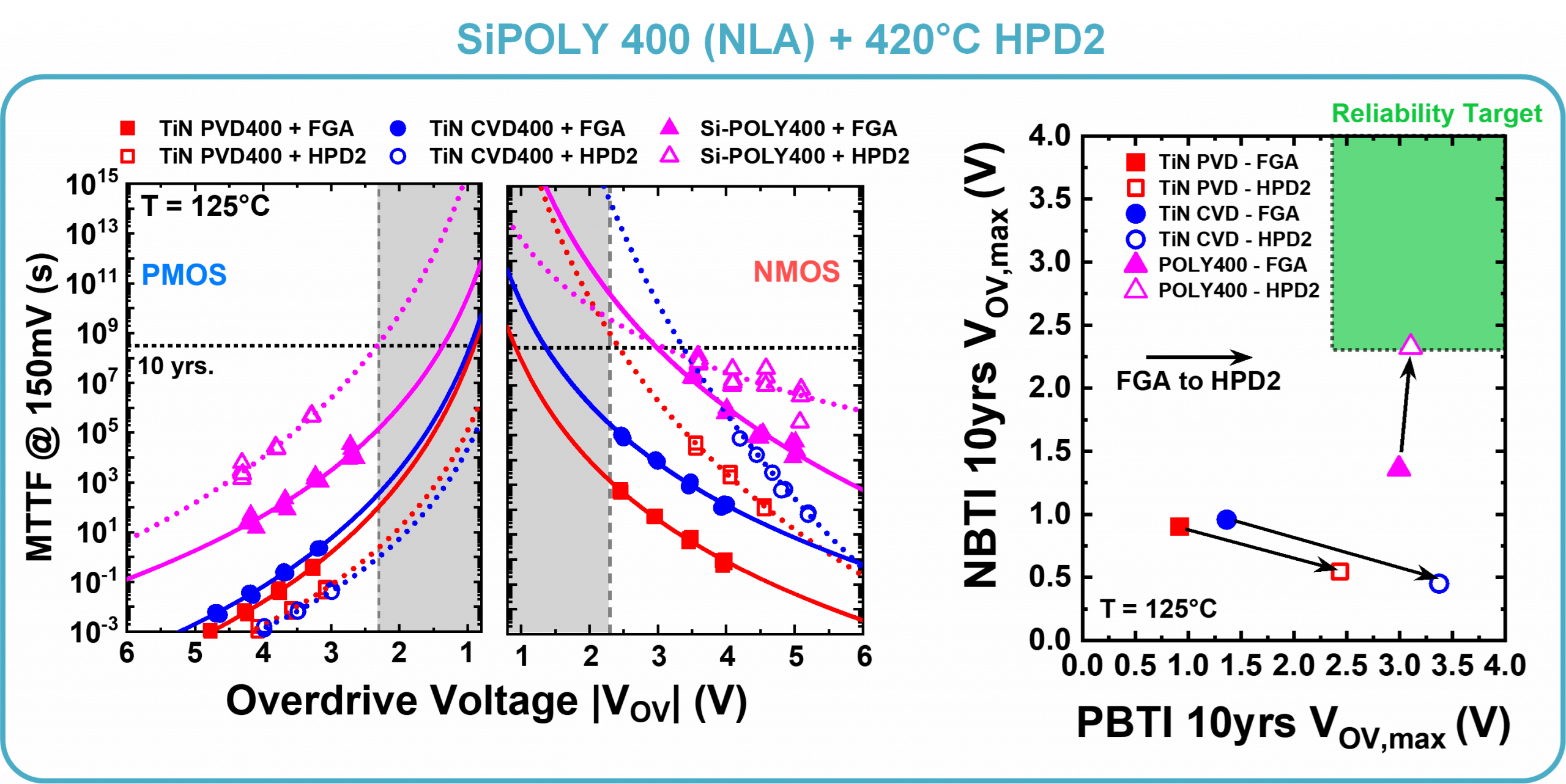
This paper investigates process options to fabricate reliable 420°C full Si CMOS high voltage transistors (reaching BTI 10yrs limit for both P/NMOS). The analysis of TiN based and Si-POLY gate with UV nanosecond laser annealing (UV-NLA), proves that TiN on SiO2 even at 420°C is not reliable due the O-scavenging (detrimental for NBTI). Si-POLY gate using UV-NLA activation with 420°C high pressure passivation (HPD2) reaches the 10yrs limit at VOV = 2.3V (VG = 2.5V) for both P/NMOS without hydrogen radical annealing (H∗), benefiting of UV-NLA fast high temperature transients. The interface traps creation during NBTI relies on gate materials concerning PMOS and, on passivation scheme for NMOS during PBTI stress. The analysis of CET maps suggests a significant reduction of H-E’ in SiO2, both for electron (-/0) and holes (0/+) traps using high pressure passivation.
William VANDENDAELE received the M.Sc. (’07) degree in nanomaterial sciences at Grenoble INP and the Ph.D. degree from University of Grenoble-Alpes (’10) in microelectronics. He joined SOITEC in 2011 where he was head of the electrical characterization of the R&D department. Between 2014 and 2023, he is in charge of the electrical characterization, tests and reliability of GaN based substrates and devices for power electronics at CEA-LETI. Since 2023, he is involved in the development of 10nm FDSOI, Low Temperature SOI and Si-Photonics technologies as a characterization and reliability expert leading a small group of engineers and students. He has authored of more than 60 papers in international conferences or journals and holds 5 patents. He has been awarded with the IEEE IRPS 2018 and 2026 best papers. He is a former member of the RSD IEEE IEDM subcommittee and current member of the IEEE IRPS Gate/MOL subcommittee and ESREF. He has been a TPC member of IWN, GaN Marathon. He serves as regular reviewer for IEEE TED, EDL and Microelectronic Reliability.