



Keynotes
Keynote I – Powering AI – Challenges and Solutions for Datacenters from a Reliability Perspective
Gerald Deboy, Infineon Technologies Austria AG, Austria
Training of ever larger and more complex AI models requires a scaling of datacenters on three levels: first, ever larger and more powerful processors, second, clustering ever more processors in close physical proximity within the IT rack and third, forming a virtual machine with 10,000 to 100,000 processors by inter-connecting every processor to every other processor. In contrast to general purpose searches, the training of AI models is hardware-centric. Each failure of one processor forces a re-start of the training from the last stored data set. With hundreds of power devices being paralleled per processor, we need to analyze failure models under realistic pulsating load patterns and strive for an unprecedented low level of failures on device level.
The talk will explore key directions for AI datacenters and discuss the resulting reliability challenges both from a system and device-level view. Redundancy, Life time models and a system-oriented reliability methodology will be required to master these challenges ahead.
Dr. Gerald Deboy is currently a Fellow with Infineon Technologies Austria AG. He serves as a System Architect for Datacenters analyzing holistically the power flow from Grid to Core. He leads a System Innovation Group focusing on fundamental building blocks for “Powering AI”.
Dr. Gerald Deboy received the M.S. and Ph.D. degree in physics from the Technical University Munich in 1991 and 1996 respectively. He joined Siemens Corporate Research and Development in 1992 and the Semiconductor Division of Siemens in 1995, which became Infineon Technologies later on. His research interests were focused on the development of new concepts for power devices based on the Superjunction principle. From 2004 onward he was heading the Technical marketing department for power semiconductors and ICs within the Infineon Technologies Austria AG. Since 2009 he is leading a System Innovation group specializing on new fields for power electronics with specific focus on application cases for wide bandgap technologies. He is a Sr. member of IEEE and has served as a member of the Technical Committee for Power Devices and Integrated Circuits within the Electron Device Society. In 2023 Dr. Gerald Deboy was awarded the IEEE Medal for Environmental and Safety Technologies jointly with co-recipients Dr. David Coe and Dr. Tatsuhiko Fujihira for contributions to concept and realization of Superjunction devices.
Dr. Deboy has authored and coauthored more than 100 papers in national and international journals including contributions to three student text books. He holds currently more than 100 granted international patents and has more applications pending.
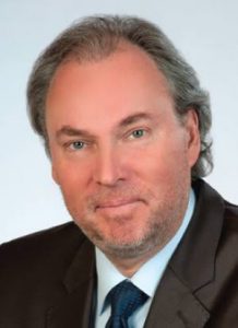
Keynote II – Technology Strategies for Evolving Compute Challenges
Ben Kaczer – imec, Belgium
The rapid proliferation of large language models and agentic AI-driven applications continue to fuel an unprecedented demand for compute across datacenters and edge systems alike. The deceleration of CMOS scaling—yielding diminishing improvements in power, performance, area, and cost (PPAC) from node to node—and the escalating costs of new designs and wafer manufacturing, present a dual challenge for compute ecosystem. Addressing these constraints requires rethinking the problem from a tops-down, system-level perspective, where new approaches beyond traditional scaling may be required. This talk will explore key bottlenecks limiting compute system performance: compute density, power delivery and efficiency, thermal management, and memory capacity and bandwidth. It will highlight emerging technology strategies to overcome these barriers – continued dimensional scaling, novel device architectures, new materials and innovative integration schemes using advanced interconnect technologies. Introduction of these options will need deeper understanding of failure modes with new reliability considerations. This will also require fresh approaches to failure modelling and system robustness to ensure sustained performance throughout the operational lifetime.
Dr. Ben Kaczer is a Scientific Director in the Advanced Reliability Robustness and Test (AR2T) department at imec. Dr. Kaczer received M.S. degree in Physical Electronics from Charles University, Prague, in 1992 and M.S. and Ph.D. degrees in Physics from The Ohio State University, in 1996 and 1998, respectively. In 1998 he joined the reliability group of imec, Leuven, Belgium, where his activities have included the research of the degradation phenomena and reliability assessment of SiO2, SiON, high-k, and ferroelectric films, planar and multiple-gate FETs, circuits, and characterization of Ge, SiGe, III-V, MIM, and TMD devices. He has co-authored more than 600 journal and conference papers with 20,000 citations (Google Scholar) and 5 patent groups related to device and circuit reliability, presented a number of invited papers and tutorials, and co-received 6 IEEE International Reliability Physics Symposium (IRPS) Best and Outstanding Paper Awards, 2 IEEE IPFA Best Paper Awards, and the 2011 IEEE EDS Paul Rappaport Award. Dr. Kaczer has served twice as the chair of the Characterization, Reliability and Yield subcommittee of the International Electron Device Meeting (IEDM; 2007 and 2015) and as a member of various subcommittees of the IRPS (2002—2016) IRPS management committee (2017—2026) and is currently serving as the General Chair of upcoming IRPS 2027. He was the General Chair of the Semiconductor Interfaces Specialists Conference (SISC; 2006) and continues to act as the conference secretary (2007—). He co-organized the INFOS conference (2005), and served on the INFOS, WoDiM, IPFA, and ICICDT conference committees. He has served on the Editorial Board of IEEE Journal of Transaction of Electron Devices for three terms (2011—2019).
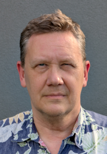
Keynote III – Integrated Workflows for Physical Failure Analysis
Tomáš Vystavěl – Thermo Fisher Scientific, Czech Republic
As semiconductor devices become more structurally complex, physical failure analysis increasingly depends on how effectively localization, site-specific preparation, and final analytical confirmation are combined into a coherent workflow. The key challenge is not only to identify the failure site, but to move efficiently from that location to reliable root-cause determination. This contribution outlines an integrated workflow for physical failure analysis, spanning localization, precision sample preparation, and high-resolution physical analysis. The focus is on how these steps work together to improve the success rate, reduce the time to answer, and increase confidence in the final diagnosis. Rather than concentrating on a particular device architecture, the contribution highlights a workflow-oriented approach that supports advanced semiconductor development and manufacturing.
Tomáš Vystavěl, is R&D Director at Thermo Fisher Scientific, where he leads architect teams developing platforms for advanced microscopy and semiconductor workflows. His background is rooted in electron microscopy and materials characterization, with extensive experience across SEM, TEM, and FIB technologies in both research and product development. He has contributed to the development of new microscopy methods and workflow solutions across multiple application areas. He currently focuses on platform and workflow development, bringing together instrumentation, software, and application expertise to support more integrated and effective solutions.