



Short Course I – Power Electronics
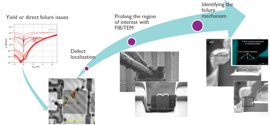
(SC1-1) Correlation of metrology data with electrical performance of lateral p-GaN HEMT devices
Izabela Kuzma-Filipek – imec, Belgium
Gallium nitride (GaN)-on-Si technology for power and RF applications requires robust defect characterization across both blanket epitaxial wafers and patterned device structures to ensure high yield, reliability, and electrical performance. A combination of optical, electron-beam, and electrical metrology techniques can provide complementary insights into defectivity at different process stages. On blanket GaN-on-Si wafers, optical inspection, photoluminescence (PL) mapping, X-ray diffraction (XRD), atomic force microscopy (AFM), and defect-selective etching are commonly employed to quantify threading dislocation density, surface morphology, stress variation, and epi-uniformity. For patterned wafers, high-resolution optical inspection, SEM review, e-beam defect inspection, scanning probe techniques, and nanoprobing enable identification of process-induced defects such as gate damage, p-GaN etch residues, metal discontinuities, particle contamination, and dielectric failures. Correlation of metrology data with electrical test results provides valuable insight into defect impact on device performance. For p-GaN HEMTs, regions exhibiting elevated threading dislocation density or abnormal PL signatures often correlate with increased off-state leakage current and reduced breakdown voltage. Localized surface defects and gate-edge process excursions detected by patterned wafer inspection have been linked to increased gate leakage, threshold voltage variation, and reduced device yield. Additionally, defect clustering identified through optical or e-beam inspection can show strong spatial correlation with wafer-level maps of dynamic RDS(on), IDSS leakage, and early reliability failures. By combining high-sensitivity defect inspection with electrical parametric and reliability characterization, a comprehensive defect-to-performance framework can be established, enabling root-cause identification, process optimization, and improved manufacturability of p-GaN HEMT technologies.
Izabela Kuzma-Filipek received her master degree (2004) in Material Engineering from AGH University of Cracow (Poland) in collaboration with EMPA Institute (Switzerland) and her Ph.D. degree (2010) in Electrical Engineering from KU Leuven Belgium. Dr. Kuzma was a Postdoctoral Researcher at the department of Si Photovoltaics at imec and subsequently senior scientist and project manager at the same department. In 2020 Dr Kuzma started new position in GaN Power Electronic department of imec as a senior researcher and project manager. Main areas of expertise: compact devices integration, failure analysis.

(SC1-2) Material systems for Power semiconductor switches
Herbert Pairitsch – Infineon Technologies Austria AG, Austria
Semiconductor switches are key components for improving the efficiency and power density of modern power electronic systems. This talk shows power switches based on different semiconductor materials, including silicon (Si), silicon carbide (SiC), and gallium nitride (GaN). In addition to material properties, the overview considers fundamentally different device concepts, particularly vertical and lateral architecture. Vertical devices offer advantages for high-voltage and high-current applications due to their scalable blocking capability and low on-state resistance. Lateral devices, in contrast, enable better System on Chip integration capability and are particularly attractive for high-frequency and integrated power applications. The different material systems provide distinct trade-offs in terms of breakdown voltage, switching speed, conduction losses, and thermal performance. Particular attention is given to the technological limits and application ranges of Si, SiC, and GaN devices including reliability aspects. The comparison demonstrates that no single semiconductor material or device concept is optimal for all power electronic applications, but the need of understanding the benefits of each for the system.
Herbert Pairitsch holds a degree in electrical engineering from the Graz University of Technology, from where he graduated in the year 1985. In 1986 he started his career at Infineon Technologies Austria AG (former Siemens HL) and held leading positions at various manufacturing and development departments. Since 2014 he served as divisional Head of R&D Funding PSS (Power and Sensor Systems). His responsibilities include the coordination of national and international research projects in the context of energy efficient electronics (e.g. LED-lighting, Smart Grids, e-Mobility) and new semiconductor materials (e.g. SiC, GaN). He held keynotes and invited talks at several conferences (e.g. IWN, PEMD, WOCSDICE, GaN Marathon).

(SC1-3) Going beyond standard characterization: optical and e-beam methods to reveal physical properties of SiC power-devices
Paul Stampfer – KAI/Infineon Technologies, Austria
Silicon carbide (SiC) power MOSFETs enable efficient switching at high voltage and temperature, yet key device-physical properties are often difficult to access with standard electrical or in-line characterization alone. This short-course lecture introduces a set of complementary “non-standard” approaches that connect optical and electron-beam observables to parameters relevant for understanding and modeling modern SiC power technologies.
- Field-effect stimulated optical spectroscopy measures light emission from fully processed SiC power MOSFETs and links the emitted photons to microscopic trapping and detrapping at the / interface with direct comparison to ab-initio defect calculations.
- Quantitative secondary-electron doping contrast in the SEM converts grayscale images into two-dimensional doping maps by exploiting potential contrast and by leveraging controlled SEM conditions such as sample bias or temperature.
- Time- and frequency-resolved EBIC (Electron Beam Induced Current) methods combine periodic beam blanking and lock-in detection in a SEM to extract and map the effective carrier lifetime locally in the space-charge region of a SiC pn-junction.

(SC1-4) Packaging of GaN devices for highest Power densities
Ali Roshanghias – Silicon Austria Labs, Austria
Although GaN devices offer superior switching speed, efficiency, and power density, the full exploitation of their capabilities is often hampered by conventional packaging technologies. This short course explores advanced interconnect and heterogeneous integration technologies for GaN packaging in both RF and power applications. It will address top-side interconnects in chip-on-board GaN micro-assemblies, ultra-fine-pitch flip-chip techniques, and 3D die stacking, highlighting how these approaches reduce parasitic effects, improve thermal management, and enable highly integrated, high-power-density GaN systems.
Dr. Ali Roshanghias is the head of the research unit for heterogeneous integration technologies at Silicon Austria Labs (SAL). He received his Ph.D. in materials science and technology in 2012. He pursued his career as a post-doc researcher in Japan and Austria in the fields of electronic materials and advanced microelectronics packaging. In 2015 he joined SAL (formerly known as CTR Carinthian Tech Research AG). He is the author of more than 100 scientific papers and patents and serves as a lecturer at the University of Klagenfurt. Ali has also served as the work package leader for integration and packaging of GaN devices in the European All2GaN project in the last 4 years.

(SC1-5) Application needs and future application roadmap including reliability aspects
Juraj Marek – Institute of Electronics and Photonics, Slovak University of Technology in Bratislava, Slovakia
GaN power switches are transforming the power semiconductor industry, driven by their superior switching speed, lower conduction losses, higher power density, and improved efficiency compared with conventional silicon MOSFETs. But this transition happens slower than originally expected. This presentation shows an overview why. The application driven demand regarding the characteristics of Power semiconductor switches is shown for various types of application. This includes also effects (e.g. short circuit robustness, or dynamic on-resistance) which are influencing system concepts. It is obvious that the choice between GaN, SiC and Si is not only decided by the application, not only by the chosen topology, but by putting all aspects together including the driving scheme (and the price). Finally, this talk will take a look into a Cristal Ball taking into account these aspects.
Juraj Marek is a scientist, expert, and deputy director at Institute of Electronics and Photonics, Slovak University of Technology in Bratislava. His main areas of expertise are oriented to diagnostics and characterization methods of power devices supported by 2D/3D electro-thermal device modeling and simulation. The results of his scientific work were published in several papers in peer-reviewed journals and in numerous international conference proceedings. He participated in numerous international and national research projects (11 EU projects, 7 national projects). Currently, he is also coordinating activities in joint project with Taiwan partner ITRI focused on development of packaging pilot line at STUBA premises for SiC and ultra-WBG devices.