


Tutorials
Tutorial I – Unlocking Material-to-System Innovation with AI
Hussam Amrouch – Technical University of Munich, Germany
We are entering a transformative era where AI is not only advancing our understanding of the world but also might revolutionize the design and development of semiconductor technologies and chip design. As technology scaling faces fundamental physical and reliability challenges, a holistic, material-to-system co-optimization approach is becoming essential. In this keynote, we explore how AI can serve as a unifying force across the semiconductor design stack—from material and device optimization to system-level implementation. We demonstrate how AI algorithms can accelerate device physics simulations, enable faster development of transistor compact modeling, and offer unprecedented speed in standard cell library characterization. We highlight how AI empowers designers, for the first time, to capture and propagate awareness of aging- and defect-related phenomena—originating at the material and device level—all the way to GDSII and final signoffs. We further discuss the critical importance of AI-driven methodologies in emerging domains such as emerging none-volatile memories and cryogen ic CMOS, where the assumptions of classical semiconductor modeling break down. Finally, we demonstrate how neural network can be effectively employed in transistor compact model offering unprecedented speedup in SPICE simulations with an accuracy error of below 0.1%.
Hussam Amrouch is Professor heading the Chair of AI Processor Design at the Technical University of Munich. He is the Founding Director of the Munich Advanced-Technology Center for AI Chips (MACHT-AI). He is the head of the Semiconductor Test and Reliability at the University of Stuttgart, Germany. He is the Academic Director of TU Munich Venture Lab for Semiconductor. He is the head of the Brain-inspired Computing at the Munich Institute of Robotics. He received his Ph.D. degree with the highest distinction from KIT, Germany in 2015. He has over 330 publications including over 135 journal articles. His multidisciplinary research covers semiconductor device physics, chip design, computer architecture. His research interest is design for reliability, AI acceleration, emerging technologies, in-memory computing, and cryogenic circuits for quantum computing. His research in AI chips and reliability have been funded by DFG, Bavarian ministry of economy, Bavarian ministry of science, Federal ministry of Science, Advantest, Infineon, and the U.S. Office of Naval Research.
Tutorial II – Reliability of Silicon-based Transistors processed at low temperatures
Xavier Garros – CEA-Leti, France
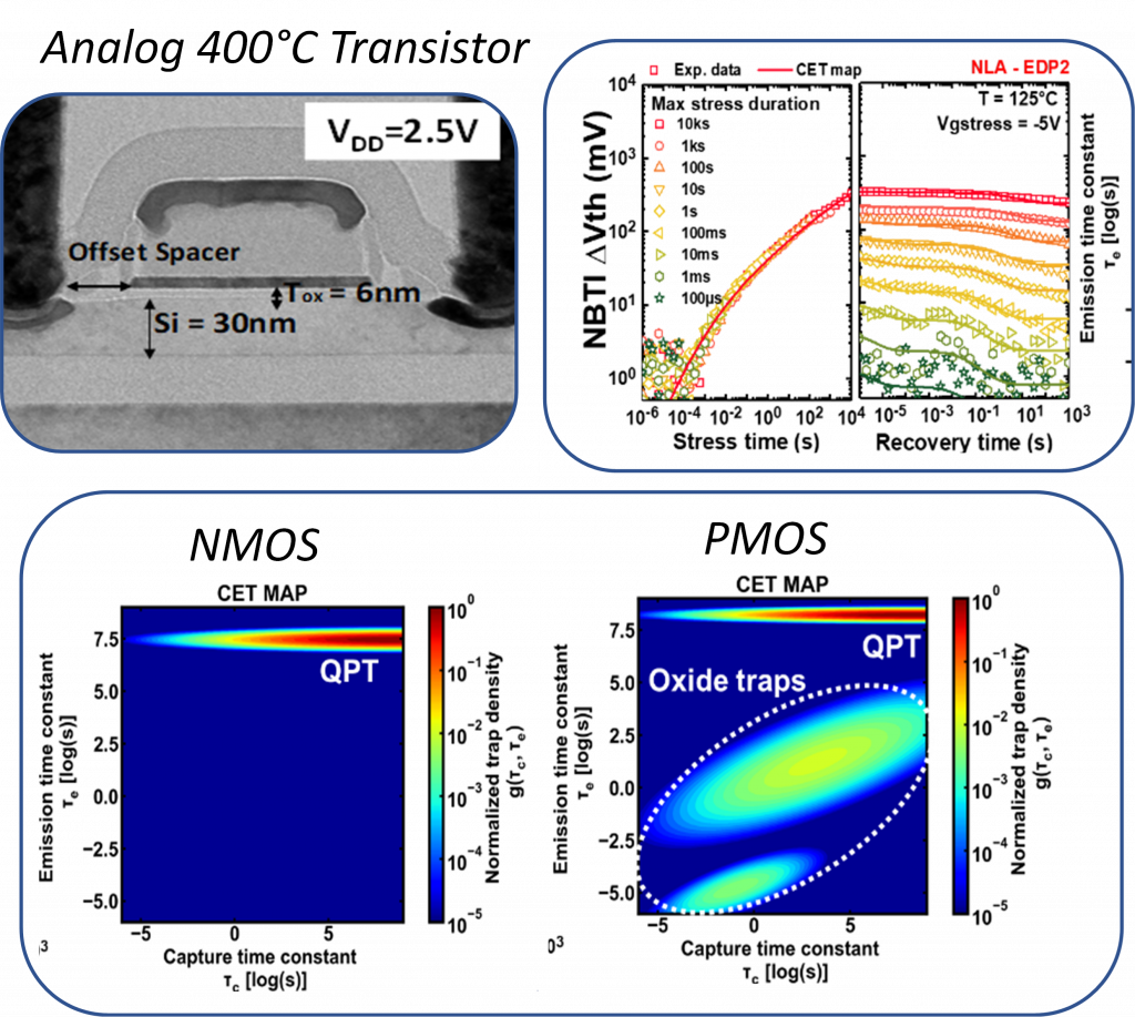
3D Sequential Integration (3DSI) is a promising alternative to continued technology scaling, enabling energy-efficient and cost-effective circuit design through the sequential stacking of active device layers. A key challenge, however, is the requirement for low-thermal-budget processing to preserve the integrity of underlying layers. This constraint raises concerns regarding the reliability of low-temperature transistors and remains a major barrier to large-scale adoption. This tutorial revisits the critical challenges associated with meeting reliability requirements for low-temperature silicon-based CMOS transistors, with a primary focus on bias temperature instability (BTI) in both n- and p-MOSFETs for digital and analog applications. A systematic investigation of the impact of thermal budget on BTI will be presented, highlighting a distinct transition in BTI behavior for processing temperatures below 600 °C. Advanced characterization and modeling techniques, including the CET map approach, will be employed to identify the oxide traps responsible for BTI in both device types. We will benchmark several process optimization strategies aimed at improving low-temperature oxide quality, including oxide growth methods, gate-stack engineering (TiN versus polysilicon), and post-deposition curing treatments such as hydrogen annealing and nanosecond laser annealing (NLA). Finally, hot-carrier reliability will be examined, with particular emphasis on the role of oxide traps in low-k spacers.
Xavier Garros is a Senior Scientist in the Silicon Technologies Department at CEA-LETI. He received his Ph.D. from the University of Marseille, France, in 2004, with a focus on the physics and electrical properties of high-k dielectrics. His expertise spans electrical characterization, device physics, and reliability modeling in advanced CMOS technologies, including bulk, FDSOI, and nanowire devices. He is currently involved in the development of 3D monolithic integration and RF technologies. He has supervised 10 Ph.D. theses and is the author or co-author of five patents and more than 160 publications in international journals and conferences in the field of CMOS physics. He has also served on the technical program committees of leading international conferences, including IEDM, IRPS, and SISC.
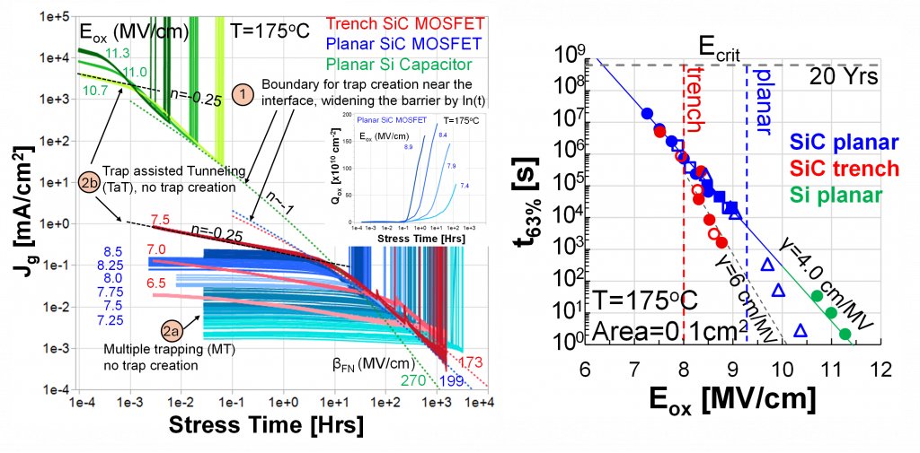
Tutorial III – Introduction to SiC power MOSFET technology and reliability
Peter Moens – onsemi Power Solutions Group, Belgium
In this tutorial we will cover the basic aspects of both planar and trench gate SiC power MOSFET device technology and their reliability. The aim is to provide the audience with insight into the status of the reliability of SiC power devices. The following topics will be addressed:
- Characterization of the SiC/SiO2 interface by charge pumping and ultra-fast BTI measurements. From the latter the capture and emission time constant maps are derived.
- Identification of the physical nature of the interface point defects through electrically detected magnetic resonance (EDMR)
- Gate Switching instability
- Gate oxide reliability (TDDB) and lifetime. Comparison of SiC/SiO2 to Si/SiO2
- Reverse bias reliability
- Cosmic ray susceptibility
- Short circuit withstanding time
- Bipolar degradation
Finally, we will provide an outlook to “Moore’s law for power devices” and where we believe SiC will be heading into the future.
Peter Moens received a Master in nuclear physics and a Ph.D. in solid state physics from the University of Gent, Belgium, in 1990 and 1993 respectively. At onsemi is working on SiC MOSFETs. He is/was a member of the technical program committees of IEDM, ISPSD, IRPS, CSMANTECH, ICSCRM, IRW, EDTM, ESSDERC and ESREF. He was the General chair of ISPSD 2012. He authored and co-authored over 200 publications in peer reviewed journals or conferences, 20 invited papers, and is the recipient of 6 best paper awards (including 2 ISPSD best paper awards as first author). He presented tutorials at IRPS, ISPSD and EDTM. He is an inductee of the ISPSD International Hall of Fame. He holds 62 US patents.